Overview
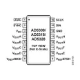
| Temperature Range | −40°c to +125°c | Package Description | 16-Lead Thin Shrink Small Outline Package (Tssop) |
| Package Option | Ru-16 | ||
Product Details
Find all the RM Microcontrollers your electronics project needs at Wachang, one of the leading manufacturers and suppliers of electronic components. Choose from our selection of MCU NXP Semiconductors, onsemi Audio Amplifiers , onsemi Image Sensors, onsemi Switching Controllers, switching controllers AC dimmer controller and MOSFET Gate Drivers at Wachang.
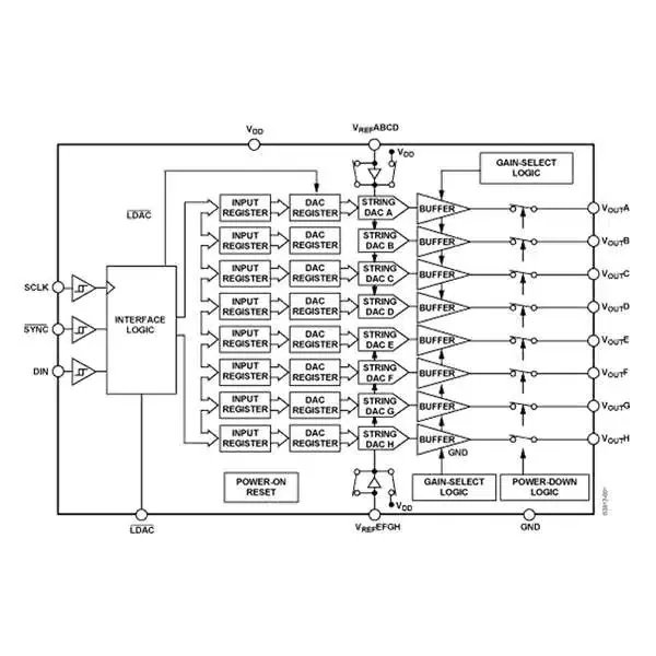
Features and Benefits AD5308: 8 buffered 8-bit DACs in 16-lead TSSOP A version: ±1 LSB INL, B version: ±0.75 LSB INL AD5318: 8 buffered 10-bit DACs in 16-lead TSSOP A version: ±4 LSB INL, B version: ±3 LSB INL AD5328: 8 buffered 12-bit DACs in 16-lead TSSOP A version: ±16 LSB INL, B version: ±12 LSB INL Low power operation: 0.7 mA @ 3 V Power-down to 120 nA @ 3 V, 400 nA @ 5 V Double-buffered input logic Guaranteed monotonic by design over all codes Buffered/unbuffered/VDD reference input options Output range: 0 V to VREF or 0 V to 2 VREF Power-on reset to 0 V
Product Details
The AD5308 / AD5318 / AD5328 are octal 8-, 10-, and 12-bit buffered voltage output DACs in a 16-lead TSSOP. They operate from a single 2.5 V to 5.5 V supply, consuming 0.7 mA typical at 3 V. Their on-chip output amplifiers allow the outputs to swing rail-to-rail with a slew rate of 0.7 V/μs. The AD5308 / AD5318 / AD5328 use a versatile 3-wire serial interface that operates at clock rates up to 30 MHz and is compatible with standard SPI, QSPI, MICROWIRE, and DSP interface standards.
The references for the eight DACs are derived from two reference pins (one per DAC quad). These reference inputs can be configured as buffered, unbuffered, or VDD inputs. The parts incorporate a power-on reset circuit, which ensures that the DAC outputs power up to 0 V and remain there until a valid write to the device takes place. The outputs of all DACs may be updated simultaneously using the asynchronous LDAC input. The parts contain a power-down feature that reduces the current consumption of the devices to 400 nA at 5 V (120 nA at 3 V). The eight channels of the DAC may be powered down individually.
All three parts are offered in the same pinout, which allows users to select the resolution appropriate for their application without redesigning their circuit board. APPLICATIONS Portable battery-powered instruments Digital gain and offset adjustment Programmable voltage and current sources Optical networking Automatic test equipment Mobile communications Programmable attenuators Industrial process control